I/O Device Driver
At this point, you have finished reading all the kernel code of egos-2000 under the grass directory. You have also finished cpu_intr.c and cpu_mmu.c under the earth directory, which handle interrupts, exceptions, and virtual memory.
In this project, you will read dev_tty.c and dev_disk.c under the earth directory. They contain the driver code for the terminal (keyboard input & screen output) and disk devices. Together, the two files have fewer than 170 lines of code, but they provide good examples of an important concept to learn in this project: memory-mapped I/O.
I/O bus and device
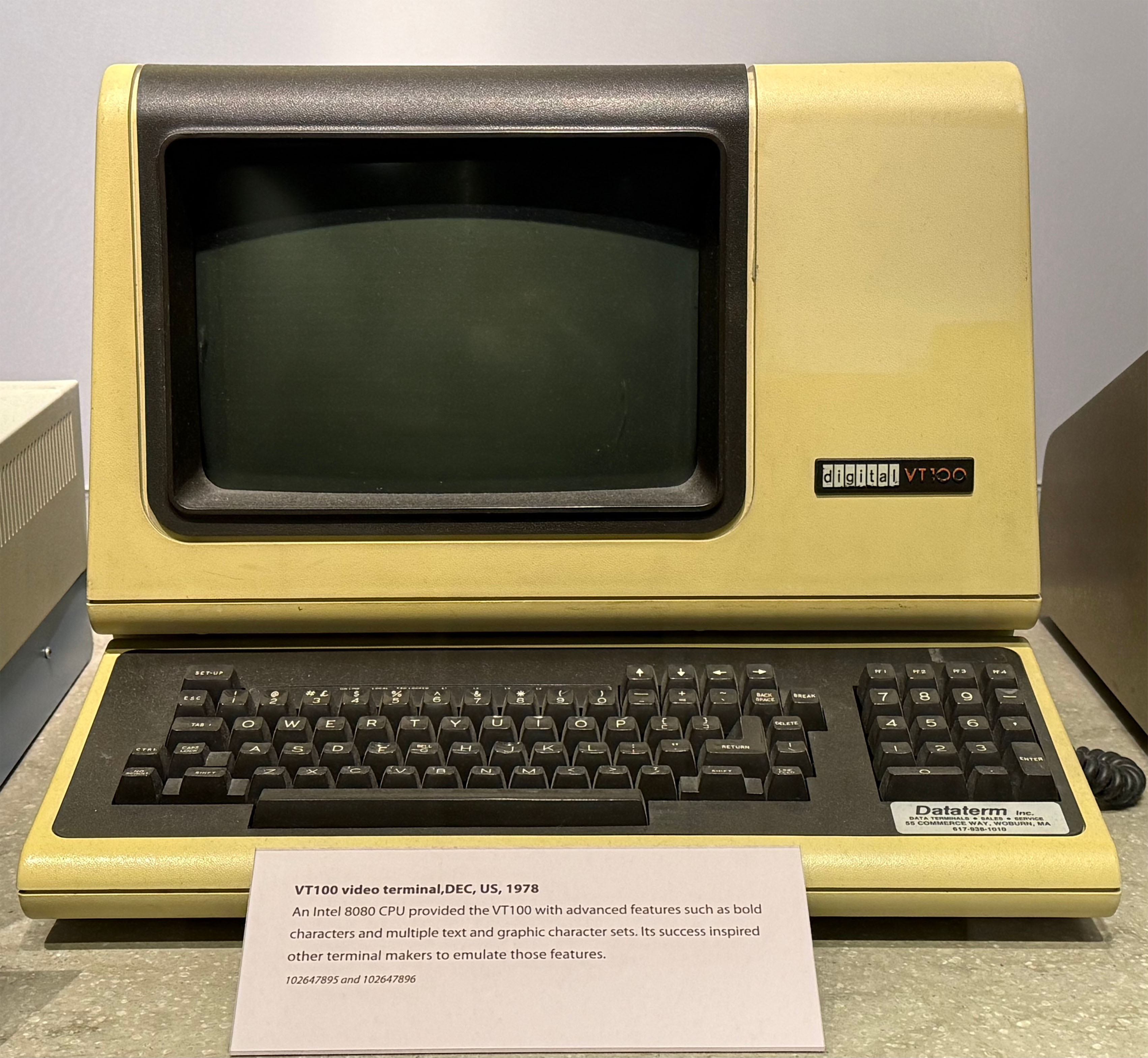
An I/O bus connects various devices to the CPU. There are different types of I/O buses, and this project introduces a few buses connecting to the terminal and disk devices. In general, computers need to read keyboard input and print characters on a screen. There used to be a separate terminal device, separate from the computer's main body, that handled these functions. This is a photo of the VT100 terminal taken at the Computer History Museum.
UART and terminal
In egos-2000, a terminal is connected to the CPU via a Universal Asynchronous Receiver/Transmitter (UART). UART uses two hardware pins on the CPU—one receiving bytes and the other transmitting (i.e., sending) bytes.
When a key is pressed on the keyboard, the terminal sends the corresponding character as a byte over UART to the CPU, and the OS reads this byte from the CPU's Receiver hardware pin. When the OS prints a character, it sends a byte through the CPU's Transmitter pin, and the UART passes the byte to the terminal. The Asynchronous in UART means that electrical signals on the two hardware pins do not wait for each other.
The code below shows how egos-2000 connects to a terminal device using UART.
#define UART_BASE   0x10000000UL
#define LINE_STATUS 5UL

void uart_getc(char* c) {
    while (!(REGB(UART_BASE, LINE_STATUS) & (1 << 0)));
    *c = REGW(UART_BASE, 0) & 0xFF;
}

void uart_putc(char c) {
    while (!(REGB(UART_BASE, LINE_STATUS) & (1 << 5)));
    REGW(UART_BASE, 0) = c;
}The CPU uses a special memory region at 0x10000000 to communicate with the terminal. When a byte is received, bit #0 of the line status register at 0x10000005 will be set to 1 by the CPU. After detecting such a byte, uart_getc reads it from address 0x10000000. When sending a byte, uart_putc waits for the UART to be idle (i.e., the previous byte has been sent) by checking bit #5 of the line status register. After the UART is idle, uart_putc writes the byte to be printed on the terminal screen to address 0x10000000.
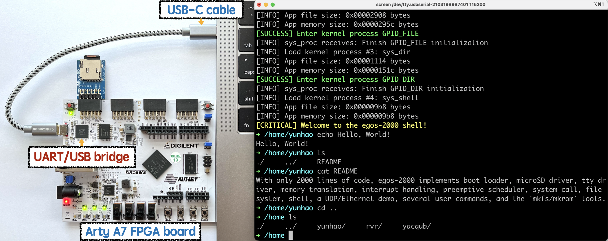
The code looks simple because most of the complexities are hidden by the hardware. For example, when running egos-2000 on a RISC-V board and using the screen command on MacOS as the terminal, the UART/USB bridge chip shown below converts electrical signals between UART and Universal Serial Bus (USB), so egos-2000 does not have to handle the complexity of USB. In real-world operating systems, the USB driver code can be much more complex than the UART code above.
This UART driver code also serves as an example of memory-mapped I/O. Specifically, a hardware manufacturer can define special memory regions for controlling I/O devices, and different manufacturers can define different regions. Indeed, egos-2000 can run on both QEMU and RISC-V boards, which use different UART regions. RISC-V boards use the region starting at 0xF0001000 to control the UART, and the driver code for RISC-V boards is also slightly different from the QEMU code in dev_tty.c.
SPI and SD card
A computer typically needs a disk to store data when powered off, and egos-2000 uses an SD card as the disk. On a RISC-V board, an SD card is connected to the CPU via the Serial Peripheral Interface (SPI), which uses four hardware pins on the CPU, as illustrated in this Wikipedia image.
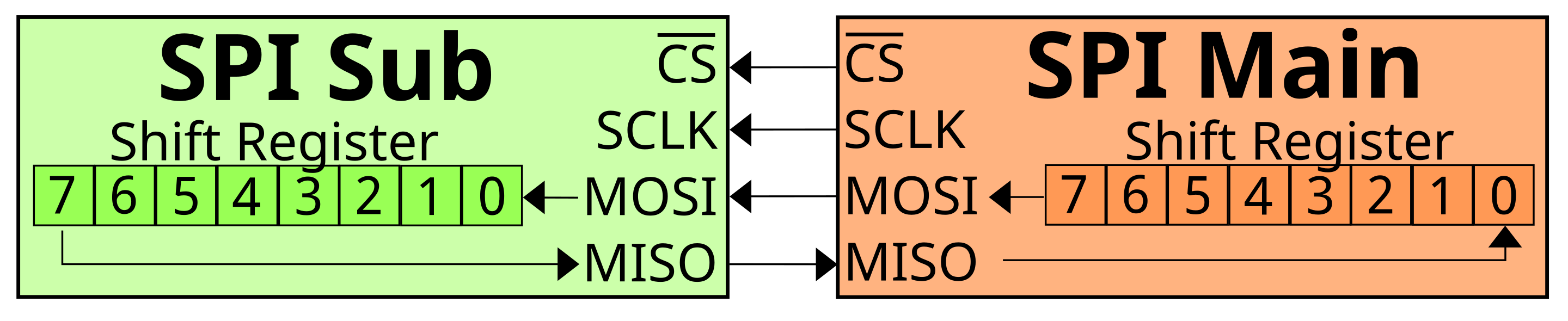
Consider the CPU as the SPI Main and the SD card device as the SPI Sub. Both sides have four hardware pins, and their functionalities are described below.
- Chip Select (CS) resets the SD card before use.
- Serial Clock (SCLK) provides clock signals from the CPU (e.g., 20MHz).
- Main Out Sub In (MOSI) is used by the CPU to send bytes to the SD card.
- Main In Sub Out (MISO) is the SD card's interface for sending bytes to the CPU.
As with UART, the CPU provides memory-mapped I/O regions for communicating with the SD card via SPI. Different from UART, the SPI Main and Sub exchange bytes synchronously during communication. The code below explains how it works.
static char spi_exchange(char byte) {
    /* The "exchange" here means sending a byte and then receiving a byte. */
    REGW(SDSPI_BASE, LITEX_SPI_MOSI)    = byte;
    REGW(SDSPI_BASE, LITEX_SPI_CONTROL) = (8 * (1 << 8) | (1));

    while ((REGW(SDSPI_BASE, LITEX_SPI_STATUS) & 1) != 1);
    return (char)(REGW(SDSPI_BASE, LITEX_SPI_MISO) & 0xFF);
}First, the byte is transmitted via the MOSI pin. Ignore LITEX_SPI_CONTROL, which is hardware-specific. After sending the byte, SPI immediately receives a byte from the MISO pin (i.e., from the SD card) as the return value of spi_exchange. The while loop waits for the arrival of a byte, just like the loop in uart_getc. SPI always receives a byte after sending one (i.e., synchronous), whereas UART is asynchronous.
While spi_exchange uses the MOSI and MISO SPI pins, the code below controls the clock signals sent out to the SCLK pin from the CPU.
#define CPU_CLOCK_RATE 100000000 /* 100MHz */
INFO("Set the SPI clock to 20MHz for the SD card");
REGW(SDSPI_BASE, LITEX_SPI_CLKDIV) = CPU_CLOCK_RATE / 20000000 + 1;TIP
As an exercise, read the sdspi_init function in dev_disk.c from which you will see how SCLK is controlled during the initialization of an SD card.
An SD card command is 6 bytes, so the operating system can ask the SD card to perform a specific task by sending the corresponding 6-byte command via spi_exchange. Given an SD card command, the sdspi_exec_cmd function sends the 6 bytes and then waits for the SD card's reply until a timeout occurs.
static char sdspi_exec_cmd(char* cmd) {
    /* Send a 6-byte SD card command through the SPI bus. */
    for (uint i = 0; i < 6; i++) spi_exchange(cmd[i]);
    #define TIME_OUT 8000
    for (uint reply, i = 0; i < TIME_OUT; i++)
        if ((reply = spi_exchange(0xFF)) != 0xFF) return reply;

    return 0xFF;
}SD card read via SPI
The SD card command #17 is defined for reading a block. An SD card block is typically 512 bytes—when reading or writing an SD card, the OS reads or writes a 512-byte block. This is different from the terminal, which reads or writes in the granularity of a single byte.
Given sdspi_exec_cmd, the sdspi_read function below reads a block from the SD card to the memory address dst, and the offset argument decides which block should be read. For example, if offset is 0, sdspi_read will read the very first block on the SD card.
static void sdspi_read(uint offset, char* dst) {
    /* Wait until SD card is ready for a new command. */
    while (spi_exchange(0xFF) != 0xFF);

    /* Send a read request with command #17. */
    char* arg = (void*)&offset;
    char reply, cmd17[] = {17 | (1 << 6), arg[3], arg[2], arg[1], arg[0], 0xFF};
    if (reply = sdspi_exec_cmd(cmd17)) FATAL("cmd17 returns status 0x%.2x", reply);

    /* Wait for the data packet and ignore the 2-byte checksum. */
    while (spi_exchange(0xFF) != 0xFE);
    for (uint i = 0; i < BLOCK_SIZE; i++) dst[i] = spi_exchange(0xFF);
    spi_exchange(0xFF);
    spi_exchange(0xFF);
}At a high level, the code above proceeds as follows.
- Wait for the SD card device to be ready for the next command.
- Send command #17 to the SD card. Out of the 6 bytes, the 4 bytes in the middle encode a block number (i.e.,
offset) indicating which block should be read. - Wait for the SD card device to be ready to send back the 512-byte block data.
- Receive 512 bytes of block data from the SD card, along with a 2-byte checksum.
We have shown a concrete example of controlling an SD card device using SPI, along with a good amount of hardware details about SPI. Next, we focus solely on the memory-mapped I/O interface because the PCIe hardware pins and signals are complex.
Plug-and-play via PCIe
While SPI provides a simple way of using an SD card, there are two constraints.
SPI devices typically need manual setup and cannot be automatically detected.
Reading the 512-byte block, byte-by-byte, through
spi_exchangeis very slow.
To address such problems, we introduce Plug-and-Play and Direct Memory Access (DMA). Plug-and-Play allows the OS to detect a new device connected to the CPU and dynamically configure memory-mapped I/O regions for it. Direct Memory Access allows the devices to read and write memory directly, so an SD card can write block data to memory without the CPU being involved (e.g., by running the loop in spi_exchange).
Plug-and-Play and DMA are enabled by the Peripheral Component Interconnect (PCI) or its successor, PCIe. In egos-2000, the memory region starting at 0x30000000 controls PCIe, which connects to multiple devices. The OS controls device #i on PCIe by reading or writing the memory region [0x30000000+0x8000*i, 0x30000000+0x8000*(i+1)). For example, the addr=0x1 in the definition of QEMU_SD_CARD in the Makefile indicates that an SD card is inserted as device #1 on the PCIe bus. Therefore, the memory at 0x30008000 is used to control this SD card (see SDHCI_PCI_ECAM in library/egos.h). Here is a table from a PCI wiki page that shows how to interpret the memory region at 0x30008000.
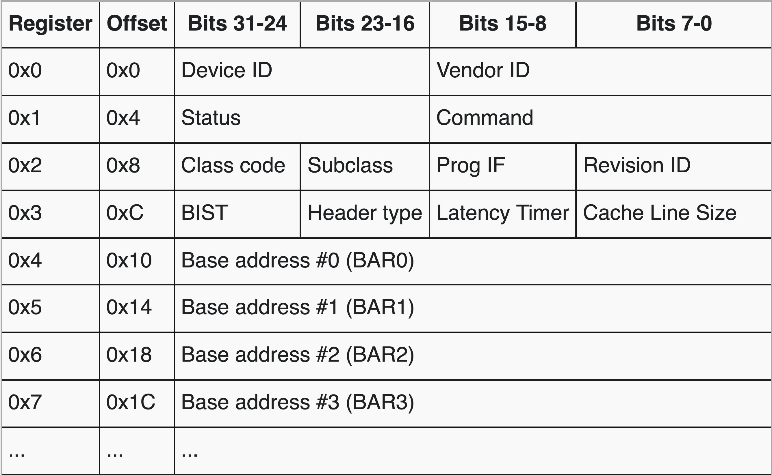
The first 4 bytes at 0x30008000 provide the Vendor ID and Device ID for device #1 on PCIe. Based on the two ID numbers, an operating system learns that device #1 is an SD card. This is essentially how Plug-and-Play works: the operating system periodically reads the 4 bytes at 0x30000000 (device #0), 0x30008000 (device #1), 0x30010000 (device #2), and so on. Using the two ID numbers, the operating system determines whether a device is plugged in or unplugged at a PCIe address. Later in this project, you will use the QEMU_GRAPHIC macro in the Makefile to plug in a VGA device as device #2 on the PCIe bus.
TIP
As an exercise, read the first two lines of the sdhci_init function in dev_disk.c. They modify Command (0x4) and Base address #0 (0x10) according to the table above. Understand these two lines of code, especially the Memory Space and Bus Master bits, by reading the PCI wiki page.
SD host controller interface
The PCIe bus provides an advanced memory-mapped I/O interface for SD cards called the Secure Digital Host Controller Interface (SDHCI). An example of using SDHCI in egos-2000 is the sdhci_read function in dev_disk.c, which reads a block via SD card command #17, just like sdspi_read, but uses direct memory access.
SDHCI specification
The SD Association maintains the official SDHCI specification, just as RISC-V International maintains the ratified RISC-V ISA specifications. In this project, you will need Chapters 2.1 and 2.2 of the SD Host Controller Simplified Specification. Table 2-1 in Chapter 2.1.1 shows the SDHCI register map, and the screenshot below shows part of this table, which is just enough to understand the sdhci_read function.

In this screenshot, 002h means 0x002—it is just a different notation for hexadecimal.
Direct memory access
The first few lines of sdhci_read prepare a direct memory access.
/* Prepare DMA (SDMA mode of SDHCI). */
static __attribute__((aligned(BLOCK_SIZE))) char aligned_buf[BLOCK_SIZE];
REGW(SDHCI_BASE, 0x0) = (uint)aligned_buf;
REGW(SDHCI_BASE, 0x4) = (1 << 16) | BLOCK_SIZE;According to the table above, the address of a 512-byte buffer aligned_buf is written to the SDMA System Address register at 000h. The Block Size register at 004h is written by BLOCK_SIZE, and the 16-bit Block Count register at 006h is written by 1. Together, these values indicate that sdhci_read asks SDHCI to write one BLOCK_SIZE-byte block to the aligned_buf buffer when executing the upcoming SD card read command.
TIP
Read the rest of sdhci_read and the sdhci_exec_cmd function by referencing the table above. The code shows how to issue SD card command #17 by writing to the Argument register at 008h, the Transfer Mode register at 00Ch, and the Command register at 00Eh. It further shows how to wait for the SD card command #17 to finish, after which the 512-byte block of data should be ready in aligned_buf, given how we have prepared the DMA.
Chapter 2.2 of the specification details all the registers in Table 2-1. You are encouraged to study the difference between Single-Operation DMA (SDMA) and Advanced DMA (ADMA) by reading more of the specification or searching online. For example, you will learn that a constraint of SDMA is that the DMA buffer cannot span across multiple memory pages. By making the DMA buffer aligned to BLOCK_SIZE, the code guarantees that the 512 bytes of aligned_buf are on the same 4KB memory page. With this constraint in mind, we now ask you to implement a better version of the SD card driver.
Multi-block read and write
Our driver code uses the SD card command #17 to read a single block, and the disk_read function simply calls sdhci_read or sdspi_read repeatedly in a loop.
The SD card standard provides commands #18 and #25 for reading and writing consecutive blocks altogether. Your job is to replace the loop in disk_read and complete disk_write with your own SD card driver using SD commands #18 and #25. They are detailed in this blog, while you can certainly find other materials about the two SD card commands online.
After you finish the new SDHCI driver, egos-2000 should run normally on QEMU. It would also be very useful and important to write unit tests for your driver code. For example, instead of booting egos-2000, you can run your unit tests right after the disk_init() in earth/boot.c. The test code should write to and read from the 4MB SD card several times and verify that the behavior is as expected. If you have a RISC-V board, you could further implement a new driver for the SPI bus using commands #18 and #25.
VGA via PCIe's plug-and-play
To learn more about device drivers, you will now plug in a VGA device on the PCIe bus and write the driver code to initialize it. The goal is to ensure that apps/user/video_demo.c can run on QEMU, as shown in this screenshot.
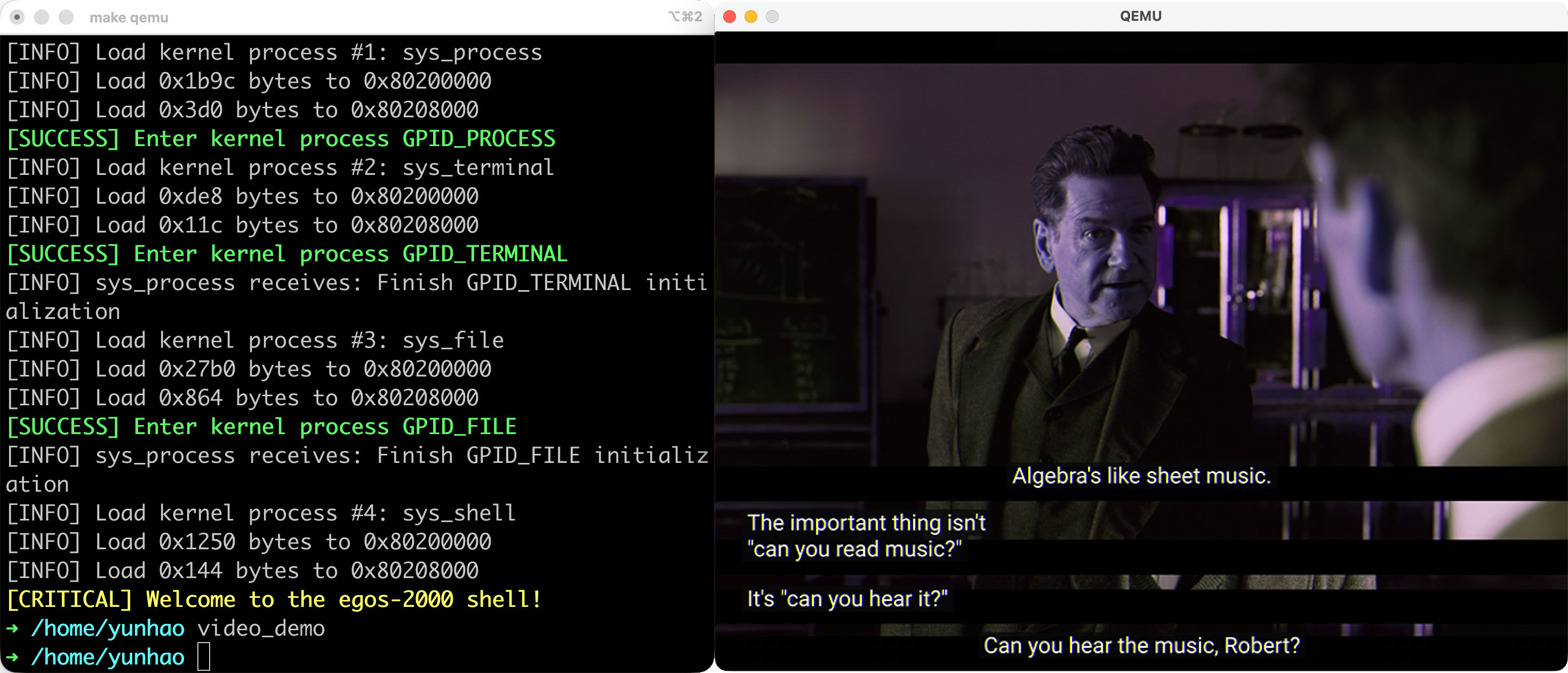
To start with, update QEMU_GRAPHIC in the Makefile to -device VGA,addr=0x2 -serial mon:stdio, which plugs in a VGA device as device #2 on the PCIe bus. The rest of your code should be in the boot() function in earth/boot.c. In QEMU's documentation for this VGA device, you can find the "PCI spec" as follows.
- PCI Region 0: Framebuffer memory, 16 MB in size (by default).
- PCI Region 2: MMIO bar, 4096 bytes in size (QEMU 1.3+)
This means you need to initialize both the base address #0 and base address #2 in device #2's PCI configuration. The first address is defined as VIDEO_FRAME_BASE in library/egos.h, and it is used by video_demo to set the RGB values of each pixel.
Your job is to pick an address for base address #2 and initialize the memory-mapped I/O region according to the "MMIO area spec" section in QEMU's documentation. The "VGA IOports" and "bochs dispi interface registers" in this section are not really well explained, so search for more information yourself. The comments in the boot() function provide some hints and guidance.
Your driver code only runs on QEMU because the VGA/HDMI device on the RISC-V boards does not require any driver code to run video_demo. If you have a board such as the $35 Tang Nano 20K and are more interested in designing a Graphical User Interface (GUI) for egos-2000, you can work on your GUI directly on the board without worrying about the VGA driver at all. You simply need a monitor and a VGA/HDMI cable or adaptor.
Accomplishments
You have learned memory-mapped I/O and three types of I/O buses by reading the device driver code in egos-2000. The SDHCI code provides examples of plug-and-play and direct memory access. You have also written your own driver for an SD card and a VGA display.